 |
| October 22, 2019 | Volume 15 Issue 40 |
Electrical/Electronic News & Products
Designfax weekly eMagazine

Archives
Partners
Manufacturing Center
Product Spotlight
Modern Applications News
Metalworking Ideas For
Today's Job Shops
Tooling and Production
Strategies for large
metalworking plants
Intro to reed switches, magnets, magnetic fields
 This brief introductory video on the DigiKey site offers tips for engineers designing with reed switches. Dr. Stephen Day, Ph.D. from Coto Technology gives a solid overview on reed switches -- complete with real-world application examples -- and a detailed explanation of how they react to magnetic fields.
View the video.
Bi-color LEDs to light up your designs
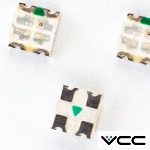 Created with engineers and OEMs in mind, SpectraBright Series SMD RGB and Bi-Color LEDs from Visual Communi-cations Company (VCC) deliver efficiency, design flexibility, and control for devices in a range of industries, including mil-aero, automated guided vehicles, EV charging stations, industrial, telecom, IoT/smart home, and medical. These 50,000-hr bi-color and RGB options save money and space on the HMI, communicating two or three operating modes in a single component.
Learn more.
All about slip rings: How they work and their uses
 Rotary Systems has put together a really nice basic primer on slip rings -- electrical collectors that carry a current from a stationary wire into a rotating device. Common uses are for power, proximity switches, strain gauges, video, and Ethernet signal transmission. This introduction also covers how to specify, assembly types, and interface requirements. Rotary Systems also manufactures rotary unions for fluid applications.
Read the overview.
Seifert thermoelectric coolers from AutomationDirect
 Automation-Direct has added new high-quality and efficient stainless steel Seifert 340 BTU/H thermoelectric coolers with 120-V and 230-V power options. Thermoelectric coolers from Seifert use the Peltier Effect to create a temperature difference between the internal and ambient heat sinks, making internal air cooler while dissipating heat into the external environment. Fans assist the convective heat transfer from the heat sinks, which are optimized for maximum flow.
Learn more.
EMI shielding honeycomb air vent panel design
 Learn from the engineering experts at Parker how honeycomb air vent panels are used to help cool electronics with airflow while maintaining electromagnetic interference (EMI) shielding. Topics include: design features, cell size and thickness, platings and coatings, and a stacked design called OMNI CELL construction. These vents can be incorporated into enclosures where EMI radiation and susceptibility is a concern or where heat dissipation is necessary. Lots of good info.
Read the Parker blog.
What is 3D-MID? Molded parts with integrated electronics from HARTING
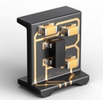 3D-MID (three-dimensional mechatronic integrated devices) technology combines electronic and mechanical functionalities into a single, 3D component. It replaces the traditional printed circuit board and opens up many new opportunities. It takes injection-molded parts and uses laser-direct structuring to etch areas of conductor structures, which are filled with a copper plating process to create very precise electronic circuits. HARTING, the technology's developer, says it's "Like a PCB, but 3D." Tons of possibilities.
View the video.
Loss-free conversion of 3D/CAD data
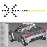 CT CoreTech-nologie has further developed its state-of-the-art CAD converter 3D_Evolution and is now introducing native interfaces for reading Solidedge and writing Nx and Solidworks files. It supports a wide range of formats such as Catia, Nx, Creo, Solidworks, Solidedge, Inventor, Step, and Jt, facilitating smooth interoperability between different systems and collaboration for engineers and designers in development environments with different CAD systems.
Learn more.
Top 5 reasons for solder joint failure
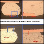 Solder joint reliability is often a pain point in the design of an electronic system. According to Tyler Ferris at ANSYS, a wide variety of factors affect joint reliability, and any one of them can drastically reduce joint lifetime. Properly identifying and mitigating potential causes during the design and manufacturing process can prevent costly and difficult-to-solve problems later in a product lifecycle.
Read this informative ANSYS blog.
Advanced overtemp detection for EV battery packs
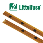 Littelfuse has introduced TTape, a ground-breaking over-temperature detection platform designed to transform the management of Li-ion battery systems. TTape helps vehicle systems monitor and manage premature cell aging effectively while reducing the risks associated with thermal runaway incidents. This solution is ideally suited for a wide range of applications, including automotive EV/HEVs, commercial vehicles, and energy storage systems.
Learn more.
Benchtop ionizer for hands-free static elimination
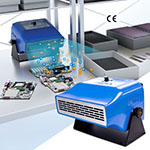 EXAIR's Varistat Benchtop Ionizer is the latest solution for neutralizing static on charged surfaces in industrial settings. Using ionizing technology, the Varistat provides a hands-free solution that requires no compressed air. Easily mounted on benchtops or machines, it is manually adjustable and perfect for processes needing comprehensive coverage such as part assembly, web cleaning, printing, and more.
Learn more.
LED light bars from AutomationDirect
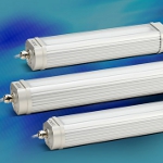 Automation-Direct adds CCEA TRACK-ALPHA-PRO series LED light bars to expand their offering of industrial LED fixtures. Their rugged industrial-grade anodized aluminum construction makes TRACKALPHA-PRO ideal for use with medium to large-size industrial machine tools and for use in wet environments. These 120 VAC-rated, high-power LED lights provide intense, uniform lighting, with up to a 4,600-lumen output (100 lumens per watt). They come with a standard bracket mount that allows for angle adjustments. Optional TACLIP mounts (sold separately) provide for extra sturdy, vibration-resistant installations.
Learn more.
World's first metalens fisheye camera
 2Pi Optics has begun commercial-ization of the first fisheye camera based on the company's proprietary metalens technology -- a breakthrough for electronics design engineers and product managers striving to miniaturize the tiny digital cameras used in advanced driver-assistance systems (ADAS), AR/VR, UAVs, robotics, and other industrial applications. This camera can operate at different wavelengths -- from visible, to near IR, to longer IR -- and is claimed to "outperform conventional refractive, wide-FOV optics in all areas: size, weight, performance, and cost."
Learn more.
Orbex offers two fiber optic rotary joint solutions
 Orbex Group announces its 700 Series of fiber optic rotary joint (FORJ) assemblies, supporting either single or multi-mode operation ideal for high-speed digital transmission over long distances. Wavelengths available are 1,310 or 1,550 nm. Applications include marine cable reels, wind turbines, robotics, and high-def video transmission. Both options feature an outer diameter of 7 mm for installation in tight spaces. Construction includes a stainless steel housing.
Learn more.
Mini tunnel magneto-resistance effect sensors
 Littelfuse has released its highly anticipated 54100 and 54140 mini Tunnel Magneto-Resistance (TMR) effect sensors, offering unmatched sensitivity and power efficiency. The key differentiator is their remarkable sensitivity and 100x improvement in power efficiency compared to Hall Effect sensors. They are well suited for applications in position and limit sensing, RPM measurement, brushless DC motor commutation, and more in various markets including appliances, home and building automation, and the industrial sectors.
Learn more.
Panasonic solar and EV components available from Newark
 Newark has added Panasonic Industry's solar inverters and EV charging system components to their power portfolio. These best-in-class products help designers meet the growing global demand for sustainable and renewable energy mobility systems. Offerings include film capacitors, power inductors, anti-surge thick film chip resistors, graphite thermal interface materials, power relays, capacitors, and wireless modules.
Learn more.
New 'electroadhesive' stamp picks up and puts down microscopic structures for assembly of circuit boards and displays
By Jennifer Chu, MIT
If you were to pry open your smartphone, you would see an array of electronic chips and components laid out across a circuit board, like a miniature city. Each component might contain even smaller "chiplets," some no wider than a human hair. These elements are often assembled with robotic grippers designed to pick up the components and place them down in precise configurations.
As circuit boards are packed with ever smaller components, however, robotic grippers' ability to manipulate these objects is approaching a limit.
"Electronics manufacturing requires handling and assembling small components in a size similar to or smaller than grains of flour," says Sanha Kim, a former MIT postdoc and research scientist who worked in the lab of mechanical engineering associate professor John Hart. "So a special pick-and-place solution is needed, rather than simply miniaturizing [existing] robotic grippers and vacuum systems."
Now Kim, Hart, and others have developed a miniature "electroadhesive" stamp that can pick up and place down objects as small as 20 nanometers wide -- about 1,000 times finer than a human hair. The stamp is made from a sparse forest of ceramic-coated carbon nanotubes arranged like bristles on a tiny brush.
When a small voltage is applied to the stamp, the carbon nanotubes become temporarily charged, forming prickles of electrical attraction that can attract a minute particle. By turning the voltage off, the stamp's "stickiness" goes away, enabling it to release the object onto a desired location.
Hart says the stamping technique can be scaled up to a manufacturing setting to print micro- and nanoscale features, for instance to pack more elements onto ever smaller computer chips. The technique may also be used to pattern other small, intricate features, such as cells for artificial tissues. The team also envisions macroscale, bioinspired electroadhesive surfaces, such as voltage-activated pads for grasping everyday objects and for gecko-like climbing robots.
"Simply by controlling voltage, you can switch the surface from basically having zero adhesion to pulling on something so strongly, on a per unit area basis, that it can act somewhat like a gecko's foot," Hart says.
The team published its results Oct. 11 in the journal Science Advances.
The team also includes Michael Boutilier, a former postdoc at MIT and now Assistant Professor at Western University in Ontario, MIT Ph.D. student Nigamaa Nayakanti, MIT postdoc Changhong Cao, and collaborators from the University of Pennsylvania, including Prof. Kevin Turner.
It's kinda like dry Scotch tape
Existing mechanical grippers are unable to pick up objects smaller than about 50 to 100 microns, mainly because at smaller scales surface forces tend to win over gravity. You may see this when pouring flour from a spoon -- inevitably, some tiny particles stick to the spoon's surface, rather than letting gravity drag them off.
"The dominance of surface forces over gravity forces becomes a problem when trying to precisely place smaller things -- which is the foundational process by which electronics are assembled into integrated systems," Hart says.
He and his colleagues noted that electroadhesion, the process of adhering materials via an applied voltage, has been used in some industrial settings to pick and place large objects, such as fabrics, textiles, and whole silicon wafers. But this same electroadhesion had never been applied to objects at the microscopic level because a new material design for controlling electroadhesion at smaller scales was needed.
Hart's group has previously worked with carbon nanotubes (CNTs) -- atoms of carbon linked in a lattice pattern and rolled into microscopic tubes. CNTs are known for their exceptional mechanical, electrical, and chemical properties, and they have been widely studied as dry adhesives.
"Previous work on CNT-based dry adhesives focused on maximizing the contact area of the nanotubes to essentially create a dry Scotch tape," Hart says. "We took the opposite approach and said, let's design a nanotube surface to minimize the contact area, but use electrostatics to turn on adhesion when we need it.'"
A sticky on/off switch
The team found that if they coated CNTs with a thin dielectric material such as aluminum oxide, when they applied a voltage to the nanotubes, the ceramic layer became polarized, meaning its positive and negative charges became temporarily separated. For instance, the positive charges of the tips of the nanotubes induced an opposite polarization in any nearby conducting material, such as a microscopic electronic element.
As a result, the nanotube-based stamp adhered to the element, picking it up like tiny, electrostatic fingers. When the researchers turned the voltage off, the nanotubes and the element depolarized, and the "stickiness" went away, allowing the stamp to detach and place the object onto a given surface.
VIDEO: New electroadhesive stamp picks and places a 170-micrometer-sized LED chiplet using an external voltage of 30V to temporarily "stick" to the LED. [Image courtesy of the researchers]
The team explored various formulations of stamp designs, altering the density of carbon nanotubes grown on the stamp, as well as the thickness of the ceramic layer that they used to coat each nanotube. They found that the thinner the ceramic layer and the more sparsely spaced the carbon nanotubes were, the greater the stamp's on/off ratio, meaning the greater the stamp's stickiness was when the voltage was on, versus when it was off.
In their experiments, the team used the stamp to pick up and place down films of nanowires, each about 1,000 times thinner than a human hair. They also used the technique to pick and place intricate patterns of polymer and metal microparticles, as well as micro-LEDs.
Hart says the electroadhesive printing technology could be scaled up to manufacture circuit boards and systems of miniature electronic chips, as well as displays with microscale LED pixels.
"With ever-advancing capabilities of semiconductor devices, an important need and opportunity is to integrate smaller and more diverse components, such as microprocessors, sensors, and optical devices," Hart says. "Often, these are necessarily made separately but must be integrated together to create next-generation electronic systems. Our technology possibly bridges the gap necessary for scalable, cost-effective assembly of these systems."
This research was supported in part by the Toyota Research Insititute, the National Science Foundation, and the MIT-Skoltech Next Generation Program.
Published October 2019
Rate this article
View our terms of use and privacy policy